导航

浏览

  • 首页
  • 中国国际半导体技术大会
  • 大讲堂
  • 招聘
首页 中国国际半导体技术大会 大讲堂 招聘
English
Richard Ali
  • 个人中心
  • Night mode
  • 退出
登录

账号密码登录

没有账号 去注册

找回密码

注册账号

已有账号 去登录

CSTIC预登记号登录

没有账号 去注册 账号密码登录

Symposium I: Device Engineering and Memory Technology

Symposium I: Device Engineering and Memory Technology

Virtual Conference Registration
  • Conference Agenda
  • CSTIC 2023 Call for Papers

Opening Remarks

  • Ru Huang

    Peking University

    View
  • Oral Session

  • Poster Session

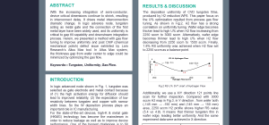
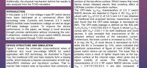
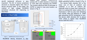
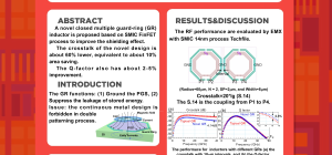
  • Solving Optimization Problems with Nanoelectronic Neuromorphic Circuits

    Dmitri Strukov

    UCSB(University of California, Santa Barbara)

    Novel Thermal Material Properties for Post-CMOS Neuromorphic Computing

    Suhas Kumar

    Sandia National Lab

    Nonvolatile-memory Based Compute-in-memory Technology for Energy Efficient DNN Accelerator

    Wonbo Shim

    Seoul National University of Science and Technology

    System-technology co-optimization for 3D monolithic memory-centric computing

    Bin Gao

    Tsinghua University

    Zinc-alloyed HfO2 synaptic RRAM with operating voltage and switching energy enhancement

    Jun Lan

    Southern University of Science and Technology

    Optimization of endurance and operation voltage in ferroelectric field effect transistor memory devices

    Kechao Tang

    Peking University

    NOVEL NEGATIVE-FEEDBACK METHOD FOR WRITING VARIATION SUPPRESSION IN FEFET-BASED COMPUTING-IN-MEMORY MACRO

    Weikai Xu

    Peking University

    A study on the Hf0.5Zr0.5O2 Ferroelectric Capacitors Fabricated with Hf and Zr Chlorides

    Jun-Fei Zheng

    Entegris Inc

    A NOVEL ANTI-FERROELECTRIC NEGATIVE CAPACITANCE TUNNELING FET WITH MITIGATED SUBTHRESHOLD SWING DEGRADATION ISSUE

    Shaodi Xu

    Peking University

    Going where silicon cannot reach: Print-in-place and recyclable electronics from nanomaterials

    Aaron Franklin

    Duke University

    Enabling 3D Monolithic Integration using Oxide-Semiconductor-based Transistors

    Xiao Gong

    National University of Singapore

    The Road to Compatible with and Beyond Silicon Circuits for 2D Materials

    Peng Zhou

    Fudan University

    Air Stable High Mobility ALD ZnO TFT with HfO2 Passivation Layer Suitable for CMOS-BEOL Integration

    Wenhui Wang

    Southern University of Science and Technology

    Low Frequency Noise of Advanced Memory and Logic Devices

    Eddy Simoen

    IMEC and University of Gent

    Study about self-heating effects in gate-all-around nanowire transistors

    Sangwan Kim

    Sogang University

    Effects of gate metal and channel shape on the variability of junctionless field-effect transistors

    Xinhe Wang

    Tsinghua University

    CFET 6T HD SRAM DESIGNS WITH 3NM DESIGN RULE

    Xiaona Zhu

    Fudan University

    Process Window Optimization of DRAM by Virtual Fabrication

    Joseph Ervin

    Lam Research

    IC Technologies and Systems for Green Future

    Min-hwa Chi

    SiEn Integrated Circuits

    Device Uniformity Improvement and Power Off Leakage Reduction by Tuning the Thickness and Profile of NMOS Work Function Metal in 28HKMG Process (PPT)

    Zhejun Liu

    HLMC

    Influence of Ion Implantation on Silicon Pits Defect Formation in Oxide Etch Process

    Zhiqiang Xiao

    Semiconductor Manufacturing North China (Beijing) Corporation(SMNC)

    Future of wafer-to-wafer bonding to overcome Non-Volatile Memory density limitations

    BELINDA DUBE

    Systemplus Consulting

    PATHFINDING BY PROCESS WINDOW CHECK: ADVANCED DRAM CAPACITOR PATTERNING PROCESS WINDOW EVALUATION USING VIRTUAL FABRICATION

    Qingpeng Wang

    Lam Research

  • Systematic Study of Temperature and VDD Impact to Read Current and Standby Leakage of SRAM in FinFET Technology

    Yijun Zhang

    SMIC

    Satellite Defects Caused by Insufficient Rinse of Lithography Development Process with A High Transmittance Mask

    WenSheng Xu

    HLMC

    T2000 ISS FT Solution Using CP Light Source

    Gong Bin

    Advantest

    A WAFER-ON-WAFER NON-UNIFORM HIGH POWER THERMAL MODEL FOR 3D CHIP PACKAGE

    Song Wang

    Xi'an UniIC Semiconductors

    AMAT High Energy Implanters Offer High Throughput and Uniformity

    Shasha Wang

    Applied Materials China

    Impact of Topology of Trench Gate Bottom Corner for Power MOSFET and IGBT

    Min-hwa Chi

    SiEN

    Investigation of removing standing wave effect during advanced litho process

    Xueqiang Liu

    HLMC

    A Novel Method using Barc EB Process to improve split gate flash erase capability

    Yaohui Zhou

    Central Semiconductor Manufacturing Corporation (CSMC)

    Optimization of Metal Line Thickness & CD and Effect on RC Delay

    PengFei Lyu

    Lam Research

    Study of HDPCVD temperature profile and its impact on IMD EM issue in 90nm CIS BEOL

    Jie Yang

    Lam Research

    Novel SOI Based Pseudo-inverter: Experimental and Simulation Research

    Sherzod Khaydarov

    Fudan university

    SIGE EPITAXIAL GROWTH ON SIGE SUBSTRATE FOR ADVANCED FDSOI TECHNOLOGY

    Yongyue Chen

    HLMC

    A PIN photodetector based on a RF-SOI substrate

    Jingjing Chou

    Fudan University

    MBIST Repair Mechanism and Implementation

    Haijing Wu

    Advantest

    EVALUATION OF DIFFERENT CUT APPROACHES ON ADVANCED BEOL SELF-ALIGNED DOUBLE PATTERNING SCHEME

    Chia Lin Lu

    Lam Research

    The Research of Decreasing SIGE Loss in Fully Depleted Silicon on Insulator (FDSOI) Devices

    Siyuan Che

    Shanghai Huali Microelectronics Corporation

    Investigation of Epoxy Molding Compound on SOP Device

    Hongjie Liu

    HHCK

    Improvement of CMOS device performance by a combination of spike and flash annealing

    KeCheng Chen

    HLMC

    Sub-20nm DRAM Metal Gate Depth Loading Improved by Advanced Pulsing Plasma Application

    Kevin Yao

    Lam Research

    Research on Vt Window Improvement Process of 55nm SONOS eFlash Cell

    Shipu Li

    Shanghai Huali Microelectronics Corporation

    Suppression of TSV Leakage of Stacking CIS by Optimizing TSV Profile and Uniformity

    Zherui Cao

    HLMC

    The effective method of enhancing WIW uniformity in Poly CMP

    Mengxia Li

    Applied Material

    ALD Characteristic Study of Al2O3 Film Deposited by a Dual Single-Wafer Process Chamber

    Ge Zhang

    Piotech Inc.

    A novel SiGe heterojunction phototransistor applicable in wide spectral range

    Yin Sha

    Beijing University of Technology

    High Quality Flatness of AP2LT Platen for HE XP penetration

    Ruijun Cui

    Applied Materials

    FCVD ANNEAL PROCESS FOR FIN CD LOSS REDUCTION STUDY

    Jun Yin

    HLMC

    Precision DARC Film Tuning to Meet DRAM D1y Customer Requirement

    Levy Wang

    Applied Materials

    The influence of the film adjustment for deep trench isolation (DTI) filling on the thermal quality in CMOS

    Yaguo Cai

    HLMC

    FDC High Order Analysis

    Yiwen He

    HLMC

    Addressable WAT test of domestic Semitronix tester

    Yangyang Xing

    HLMC

    40nm backside optimization and improvement

    Lu Xu

    HLMC

    37nm Defect Reduction Study for ILD CMP of 14nm FinFET Process

    Yunhong Hou

    Applied Materials

    A Study of LDMOS with High Breakdown Voltage and Low On-Resistance in 22nm Technology

    Zhenchao Sui

    Semiconductor Manufacturing North China (Beijing) Corporation(SMNC)

    A study of the effect of SiGe on the inverse narrow width effect in 28nm Process

    Yang Li

    HLMC

    Improving the Device Performance of LDMOS through the Optimization of Structure

    Shuang Jiao

    HLMC

    Bottom dielectric isolation to suppress sub-fin parasitic channel of vertically-stacked horizontal gate-all-around Si nanosheets devices

    Lei Cao

    Institute of Microelectronics of Chinese Academy of Sciences and University of Chinese Academy of Sciences

    Influence of Parasitic Capacitance and Resistance on Performance of 6T-SRAM for Advanced CMOS Circuits Design

    Yanna Luo

    Institute of Microelectronics of the Chinese Academy of Sciences

    Methods of Reducing Etching Residue Defects in Back End of Line for Semiconductor in 28nm Technology

    Shanshan Chen

    Shanghai Huali Integrated Circuit Corporation

    EVO head for CMP planarization improvement in advanced wafer house

    Chienchung Li

    Applied Materials

    Applied ALD SiN solutions to improve device mobility in advance DRAM

    Ze Yuan

    Applied Materials

    Hard Mask Open Tilting Improvement with Advanced Source Coil

    Xiantao Luo

    Applied Materials

    W Deposition Uniformity improvement with gas flow tuning

    Bruce Fan

    Lam Research

    Optimization and Demonstration of Low-Voltage NMOS for RF Switch Application in 65nm SOI Technology

    Zhaozhao Xu

    Huahong Semiconductor (Wuxi) Limited

    Study of Breakdown Voltage improvement of High-voltage NLDMOS in width direction

    Wenting Duan

    HuaHong Grace Semiconductor Manufacturing Corporation

    Low crosstalk and high Q-factor inductor based on multiple guard-ring design

    Xiaodong Wang

    SMIC

    Flicker noise characterization of LDMOS in FinFET technology

    Yuning Guo

    SMIC

    LOW ON-RESISTANCE LDMOS WITH STEPPED FIELD PLATES FROM 12V TO 40V IN 300-MM 90-NM BCD TECHNOLOGY

    Zhaozhao Xu

    Huahong Semiconductor (Wuxi) Limited

Sponsors:

© 2022 SEMI 云官网. All Rights Reserved.

30