导航

浏览

  • 首页
  • 集成电路科学技术大会
  • 大讲堂
  • 招聘
首页 集成电路科学技术大会 大讲堂 招聘
English
Richard Ali
  • 个人中心
  • Night mode
  • 退出
登录

账号密码登录

没有账号 去注册 CSTIC预登记号登录

找回密码

注册账号

已有账号 去登录

CSTIC预登记号登录

没有账号 去注册 账号密码登录

Symposium III: Dry & Wet Etch and Cleaning

Symposium III: Dry & Wet Etch and Cleaning

Virtual Conference Registration
  • Conference Agenda
  • CSTIC 2023 Call for Papers

Opening Remarks

  • Oral Session

  • Poster Session

  • How Process, Equipment, Material, Computation that work together to make up the Performance of Photolithography
    Qiang Wu

    Fudan University
    Novel Etch Solution with Sym3 for Logic BEOL Patterning Etch Applications

    Hui Sun

    Applied Materials

    New Materials and New Functionalities Co-work scaling, and the Exploration of Inner Spacer Technique

    David Xiao

    Qianmo Micros Design LLC

    Study of tungsten-doped carbon hard mask etch using O2/NF3 based chemistry

    Li-Tian Xu

    Beijing NAURA Microelectronics Equipment Co., Ltd.
    Plasma Corrosion Resistant ALD Coatings for Semiconductor Manufacturing Process Equipment

    Lassi Leppilahti

    Beneq

    A Study on SADP Film Stack Selection for Line Roughness Improvement in Planar 1xnm NAND Flash

    Yinan Ma

    Semiconductor Manufacturing North China (Beijing) Corporation

    A STUDY OF WAFER-LESS AUTO CLEAN EFFICIENCY PROMOTION METHOD IN DOUBLE PATTERNING DIELECTRIC HARD MASK PROCESS

    Xinruo Su

    Semiconductor Manufacturing North China

    Challenge of boron-doped silicon hardmask etching

    Xuehua Wang

    Beijing NAURA Microelectronics Equipment Co., Ltd.

    Precise etching technology of ultra thin Al2O3 film using BCl3 chemistry

    Cheng Tian

    Beijing NAURA Microelectronics Equipment Co., Ltd

    New development of ICP etching for advanced patterning

    Zhongwei Jiang

    Beijing NAURA Microelectronics Equipment Co., Ltd.
    The challenges and new developments on TSV etch applications

    Guorong Li

    Beijing NAURA Microelectronics Equipment Co., Ltd.

    High aspect ratio carbon hardmask etch process for profile and LCDU control

    Mengjiao Zhu

    Beijing NAURA Microelectronics Equipment Co., Ltd.
    Line edge roughness reduction in high aspect ratio carbon hardmask patterning for slit trench

    Li Zeng

    Beijing NAURA Microelectronics Equipment Co., Ltd.

    Challenges of Inductively Coupled Plasma Applications

    Hu Zhou

    Advanced Micro-Fabrication Equipment Inc. China

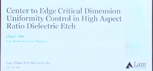
    Center to Edge Critical Dimension Uniformity Control in High Aspect Ratio Dielectric Etch

    Jiayu Sun

    Lam Research

    Profile Control for BEOL Tri-layer Patterning Scheme

    Xingxing Xu

    Lam Research

    Plasma etching solutions for compound semiconductors

    Yali Fu

    Beijing NAURA Microelectronics Equipment Co., Ltd.
    The New Developments in Etching of Dielectrics

    Yuanwei Lin

    Beijing NAURA Microelectronics Equipment Co., Ltd.

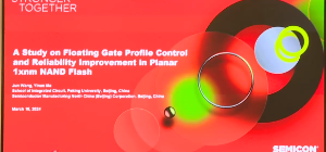
    A Study on Floating Gate Profile Control and Reliability Improvement in Planar 1xnm NAND Flash

    Jun Wang

    Peking University

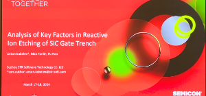
    Analysis of Key Factors in Reactive Ion Etching of SiC Gate Trench

    Anton Kobelev

    Suzhou STR Software Technology Co., Ltd.
    Ultra low temperature high aspect ratio OX punch through etching

    Hanlin Cui

    Applied Materials

  • Sidewall kink elimination of slanted gratings utilizing a twice-etching method

    Jiuru Gao

    Jiangsu Leuven Instruments Co. Ltd
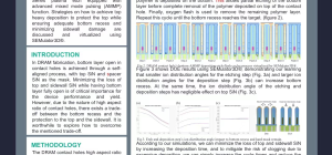
    Optimized AMMP for High Aspect-Ratio Bottom Contact Open Process in DRAM Applications

    Rick Yang

    Residue Improvement in Liner OX Open Process

    Ruxun Yuan

    Lam Research

    A STUDY ON THE DIFFERENT APPROACHS OF DUMMY GATE WET REMOVAL APPLICATION

    Tianhao Zhang

    Lam Research

    Mandrel/Non-Mandrel Imbalance Improvement for Self-aligned Reverse Patterning Process

    Shiming Zhang

    Lam Research

    Improvement of Outer Hole Profile Bending in High Aspect Ratio Dielectric Hole Etching

    Taojun Zhuang

    Lam Research

    Improved Si Grass Control during Profile tuning for Silicon Trench Etch in Power MOSFET

    Xi Chen

    Lam Research

    Profile Controlling in High Aspect Ratio Si Trench Etching by Steady-State-Process

    Yaming Liu

    Lam Research

    Ultra-Deep via Etching of Silicon Oxide for High-Voltage Capacitive Isolators

    Yuyan Xia

    Zhejiang University

    Optimization of the Polysilicon Gate Etching Process in SONOS Memory Fabrication

    Wanli Yang

    Zhejiang University

    Defect Improvement in Process Containing SiOx Passivation

    JunMing Wang

    Lam Research

    Improvement of Line Roughness of Fin by Conventional Thermal Oxidation and Atomic Level Low-Temperature Ozone Treatments

    Peng Wang

    Integrated Circuit Advanced Process R&D Center Institute of Microelectronics of the Chinese Academy of Sciences
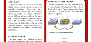
    Reaction temperature impact on Siconi® process

    Songtao Lv

    applied materials

    MTBC Enhancement through new WET Clean implement for preventing wafer breakage

    Chunlong Qiu

    Applied Materials

    A low-cost solution for Selectra™ Si Chamber Etch rate drift

    Jing Cao

    Applied Materials

    TiN Hard Mask Open Comprehensive Study

    Shuda Xu

    Applied Materials

    Improvement of CIS TM Profile by Adjusting Gas Ratio

    Ziyue Xuan

    Applied Materials

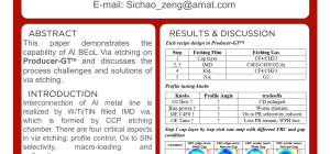
    Al BEoL Via Etching Challenge and Solution on Producer-GT™

    Sichao Zeng

    Applied Materials

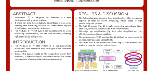
    Producer-GT™ High Productivity CCP Etch Solution

    Xipeng Tong

    Applied Materials

    Application of Hardware and Process Fine Tune for Chamber Matching in DRAM Critical Etch

    Nick Fang

    Lam Research

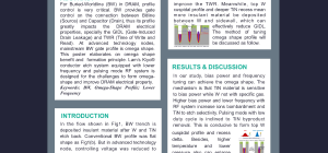
    Buried-Worldline Omega-Shape Profile Control and Impact in DRAM

    Liubo Ma

    Lam Research

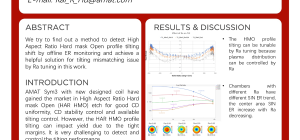
    HAR HMO tilting offline monitor and chamber to chamber matching solution

    Kai Hu

    Applied Materials

    Methods of Profile Control in HVCAP VIA Etching

    Tongyao Zhao

    Applied Materials

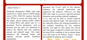
    Profile Control of CIS BVia Silicon Etch

    Le Jiang

    Applied Materials

    Advanced Mixed Mode Pulsing in DRAM Active Area Etch

    Zheng Ruan

    Lam Research

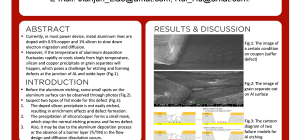
    A Study of Al etch process defects

    Jiajie Li

    Applied Materials

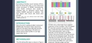
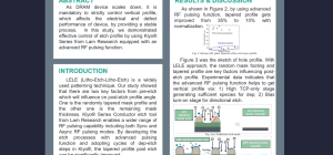
    Advanced Pulsing in LELE Application for Controllable Profile

    Hui Xu

    Lam Research

    300mm AL(0.5%Cu+1%Si) Etch Challenge and Solution on Advantage Edge Metal™

    Jianjun Liao

    Applied Materials

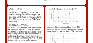
    TiN selectivity improvement for All-in-one Etch

    Yifeng Xu

    Applied Materials

    BCD process contact-etch challenges and solutions at Producer GT

    Gang Sheng

    Applied Materials

    Study of A-Si as Dry Etch Hard Mask in BEOL Low-k Dielectric Patterning

    Juxin Yin

    Zhejiang University

    Study on Integrated Trench Etching for Trench-Type Power MOSFET

    Jingru Shen

    Zhejiang University

    An approach to achieve a flat bottom in Si trench with oxide & poly pillar

    Wei Gu

    Applied Materials

    Approaches of Pitch Walking Improvement in SAQP Patterning

    Rishuai Zheng

    Applied Materials

    A Method of VIA Etch CD Range Improvement

    Qunfeng Wen

    Applied Materials

    Effect of Low Damage Strip on Si and SiGe Surface State

    Shijing Wang

    Shanghai AnBang Semi Equipment Co., Ltd
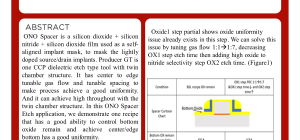
    Oxide Remain Control for BCD ONO Spacer Etch on AMAT Producer GT_Wang Miao_Etch

    Miao Wang

    Applied Materials

    Excellent Profile Control for Micro-OLED Anode Etch

    Lijun Shan

    Applied Materials

© 2022 SEMI 云官网. All Rights Reserved.

32