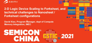
2-D Logic Device Scaling to Forksheet, and Technical Challenges to Nanosheet / Forksheet Configurations
David Xiao
IMEC
David Xiao
IMEC
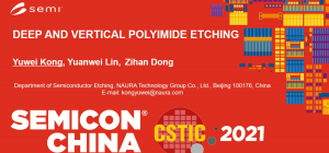

Yuwei Kong
NAURA


Yoshihide Kihara
TEL

Jianping Zhao
TEL
Bo Zhang
HHGrace
Abin Shin
AMEC

Yuanwei Lin
NAURA

Patrick Duchi
Inventec Performance Chemicals

Ping Linda Zhang
Richmond Star Hi-Tech Consulting Inc.

Zhongwei Jiang
NAURA

Peter Ventzek
TEL, US

zoushifeng
HHGrace
Zhuo Yin
Peking University
Tianyin Sun
Lam Research
Chien-Pin Sherman Hsu
Avantor
Hexin Zhou
Lam Research
Biran Zhang
Applied Materials (China), Inc.
Sun Li Fei, Wang Qing Peng, Zhang Ji Hong, Chi Yu Shan
Lam Research
PengFei Lyu
Lam Research Service Co., Ltd
Sun Yiling
Lam Research Corporation
Caigan Chen
Lam Research Service Co. Ltd.
Caigan Chen
Lam Research Service Co. Ltd.
Quanbao Li; Xiaohui Ren; Jihong Zhang; Yushan Chi
Lam Research Service Co., Ltd
Xiaohui Ren
Lam Research Service Co., Ltd
Jia Xu
Lam Research
Pin Chang, Li
Lam Research
Yongjie Hu
Jiangsu Normal University
Junming Wang
Lam Research
Chun Gao
Lam Research
Tao, Ye
Lam Research
Yan He
NAURA