Advanced Packaging Architectures for Advanced Heterogeneous Integration (HI)

Ravi Mahajan
Intel

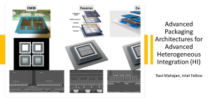
Ravi Mahajan
Intel


TORU FUJIMORI
FUJIFILM Corporation
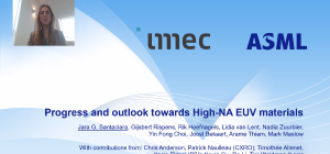

Jara Garcia Santaclara
ASML
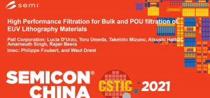

Lucia D’Urzo
Pall


Runhui Huang
Brewer Science Inc.


AO CHEN
Mentor, a Siemens Business

Rui Hu
ICRD
Yan Yan
ICRD

Qian Xie
Mentor, a Siemens Business


Leo Pang
D2S

Yongqiang Hou
ICRD

Hakaru Mizoguchi
Gigaphoton

Stephen Renwick
Nikon Research Corp of America

Keita Sakai
Canon Inc.

Huigao Duan
Hunan University

Xue Huang
YMTC

Peter Henriksson
Mycronic AB

Masami Ikota
Hitachi High-Tech Corp.


Masahiko OKUMURA
Nikon Corporation
Hao Jiang
Huazhong University of Science and Technology


Chen Lijun
Shanghai Huali Microelectronics Corporation

Zheng Haichang
Shanghai Huali Microelectronics Corporation

Li Chen
Shanghai IC R&D Center

Minxiang Wang
Lam Research Service Co., Ltd

Zhou Tao
Shanghai IC R&D Center