导航

浏览

  • 首页
  • 中国国际半导体技术大会
  • 大讲堂
  • 招聘
首页 中国国际半导体技术大会 大讲堂 招聘
English
Richard Ali
  • 个人中心
  • Night mode
  • 退出
登录

账号密码登录

没有账号 去注册 CSTIC预登记号登录

找回密码

注册账号

已有账号 去登录

CSTIC预登记号登录

没有账号 去注册 账号密码登录

Symposium II: Lithography and Patterning

Symposium II: Lithography and Patterning

Virtual Conference Registration
  • Conference Agenda
  • CSTIC 2023 Call for Papers

Opening Remarks

  • Oral Session

  • Poster Session

  • Lithography Material Challenge

    Allen Chang

    JSR, Taiwan
    Co-advancing Scaling Techniques and Functionality Enhanced Potential Device Infrastructures

    David Xiao

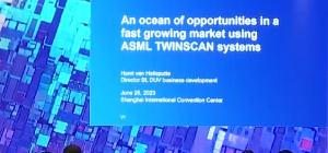
    An ocean of opportunities in a fast growing market using ASML TWINSCAN systems

    Henri van Helleputte

    ASML Netherlands B.V.
    A Positive-Tone Photosensitive Polyimide Material for Semiconductor Packaging

    Yongqiang Wang

    Jinan ShengQuan New Materials Limited

    Recent progress of EUV resist development for improving Chemical Stochastic

    TORU FUJIMORI

    FUJIFILM Corporation

    From micro to nano, and beyond, --- Measuring Innovations ---

    Zhigang Wang

    Hitachi High-Tech Corporation

    Modification of Organic Underlayer by Plasma During Dry Etching and its Effect on the Film Properties

    Soojung Leem

    DuPont Electronics & Industrial

    CycleGan-based mask diffraction model

    Yijiang Shen

    Guangdong University of Technology
    Illumination optimization for the BEOL DTCO with 45 degree local interconnection

    Xianhe Liu

    Fudan University, School of Microelectronics

    Process and tool monitor and diagnosis based on overlay data and modeling

    Yi Tong

    Guangdong Greater Bay Area Institute of Integrated Circuit and System, Guangzhou, China
    The Analysis of Optical Critical Dimension Signal Strength Between 5 nm FinFET and 3 nm CFET Vertical Gate Stacks

    Qi Wang

    Fudan University

    The Possibility of Using 193 nm Immersion Lithography Process for 5 nm Logic Design Rules

    Qiang Wu

    Fudan University

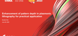
    Enhancement of pattern depth in plasmonic lithography for practical application

    Dandan Han

    University of Chinese Academy of Sciences
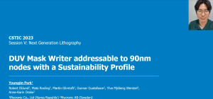
    DUV Mask Writer addressable to 90nm nodes with a Sustainability Profile

    Youngjin Park

    Mycronic Co., Ltd.

    Patterned wafer defect inspection at advanced technology nodes

    Jinlong Zhu

    HUST

  • Study on inter-layer overlay of stitching lithography technology

    Hongmin Liu

    SMIC

    A Negative-tone Photosensitive Epoxy Material

    Ke Bai

    Shandong Shengquan New Materials Co. Ltd.

© 2022 SEMI 云官网. All Rights Reserved.

31