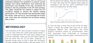
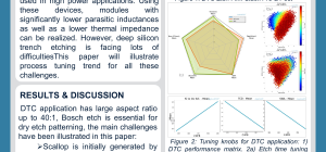
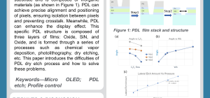
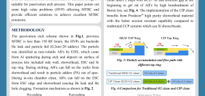
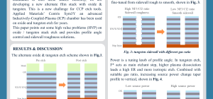
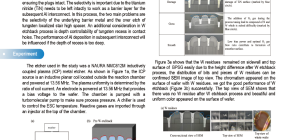
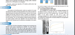
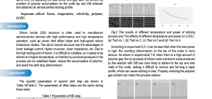
From "Iso-Dense" Biasing to "Inverse Lithography:" Milestones in Optical Proximity Correction Technology

Michael Rieger
Synopsys(retired)
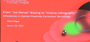
Michael Rieger
Synopsys(retired)
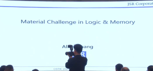
Allen(Cheng Yao) Chang
JSR
David Xiao
Qianmo Microelectronics

Hongbo Sun
Beijing Chaoxian Memory Research Institute

Chia Lin Lu
Applied Materials

Fansheng Wang
Applied Materials China
Masaru Izawa
Hitachi High-Tech Corporation

Jiasheng Sun
Suzhou Youlun Vacuum Equipment Technology Co., Ltd.
Zhongwei Jiang
Beijing NAURA Technology Group Co., Ltd.

Li Fei Sun
Lam Research

Chao Lv
Beijing NAURA Technology Group Co., Ltd.

Shijing Wang
Shanghai BangXin Semi Technology Co., Ltd.

Yuxuan Zhai
Institute of Microelectronics, Chinese Academy of Sciences

Lei Sun
Applied Materials China

Ling Wang
Ferrotec Technology Development (Shanghai) Co. Ltd

Jun Luo
Beijing NAURA Technology Group Co., Ltd.
Yang Ding

Litian Xu
Beijing NAURA Technology Group Co., Ltd.

Yuxing Yang
Jiangsu Leuven Instruments Co., Ltd.

Jiao Jin
Beijing Superstring Academy of Memory Technology

Yoshiaki Yamada
Hangzhou Cobetter Filtration Equipment Co.,Ltd


Ahmad Hassan Siddique
Tsinghua University

Chenming Xu
Jiangsu Leuven Instruments Co., Ltd.

Chengxi Yao
Sungkyunkwan University

Zehua Hei
Beijing Superstring Academy of Memory Technology

Licheng Yang
Beijing NAURA Technology Group Co., Ltd.

Haiyang Lv
Advanced Micro-Fabrication Equipment Company Inc.

Fan Yu
Beijing NAURA Technology Group Co., Ltd.

Anton Kobelev
Suzhou STR Software Technology Co., Ltd

Chaoyang Guan
Beijing Superstring Academy of Memory Technology

Taojun Zhang
Jiangsu Leuven Instruments Co., Ltd.

Chun Gao
Lam Research

Quanzhi Long
Zhejiang University

Zhanduo Bai
Semiconductor manufacturing International (Beijing) Corporation

Yuying Liu
Lam Research

Xin Su
Advanced Micro-Fabrication Equipment Company Inc.

Jiahui Sun
Beijing Superstring Academy of Memory Technology

Jianhang Chen
Nexchip Semiconductor Corportion

Weiming Liu
Advanced Micro-Fabrication Equipment Inc.

Yang Wei
Nexchip Semiconductor Corporation


Gui Cong
Nexchip Semiconductor Corporation

Xuan Liu
Semiconductor Manufacturing North China (Beijing) Co.,Ltd.

Sichao Zeng
Applied Materials China

Jie Wang
Applied Materials China

Tianyuan Liu
Applied Materials China

Xipeng Tong
Applied Materials China

Long Men
Applied Materials China

Wang Miao
Applied Materials China

Le Jiang
Applied Materials China

Fan Zhou
Applied Materials China

Kai Hu
Applied Materials China

Qunfeng Wen
Applied Materials China

Zhang Weiqiang
Applied Materials China


Chunlong Qiu
Applied Materials China

Songtao Lv
Applied Materials China

Difan Li
Applied Materials China

Bao Jing
Applied Materials China

Jianjun Liao
Applied Materials China

Kairong Cui
Applied Materials China

Fan Chen
Applied Materials China

Ping Zheng,
Applied Materials China

Jimmy Fu
Applied Materials China

Lijun Shan
Applied Materials China

Tongyao Zhao
Applied Materials China

Jing Cao
Applied Materials China

Shuda Xu
Applied Materials China

Ziyue Xuan
Applied Materials China

Hanlin Cui
Applied Materials China

Longjie Yu
Applied Materials China

Caili Lang
Applied Materials China

Jiajie Li
Applied Materials China

Wenyi Tang
Applied Materials China

Lin Luo
Applied Materials China


Dongjiang Wang
Applied Materials China

Rishuai Zheng
Applied Materials China

Zheng Ruan
Lam Research

Kevin Yao
Lam Research

Shipeng Gong
Lam Research

Rui Hu
Applied Materials China

Haoran Song
Beijing NAURA Technology Group Co., Ltd.


Mengjiao Zhu
Beijing NAURA Technology Group Co., Ltd.

Li Zeng
Beijing NAURA Technology Group Co., Ltd.

Xuehua Wang
Beijing NAURA Technology Group Co., Ltd.


Yiman Ma
Beijing NAURA Technology Group Co., Ltd.


Guangzhao Yuan
Beijing NAURA Technology Group Co., Ltd.

Yu Hao
Beijing NAURA Technology Group Co., Ltd.

Teng Zhang
Beijing NAURA Technology Group Co., Ltd.

Run Zhang
Beijing NAURA Technology Group Co., Ltd.

Shun Yang
Beijing NAURA Technology Group Co., Ltd.

Yingjie Wang
Beijing NAURA Technology Group Co., Ltd.

Yiming Ma
Beijing NAURA Technology Group Co., Ltd.

Guohui Jia
Beijing NAURA Technology Group Co., Ltd.

Chao Xu
Beijing NAURA Technology Group Co., Ltd.

Xiaoxia Meng
Advanced Micro-Fabrication Equipment Company Inc.

Yue Wei
Advanced Micro-Fabrication Equipment Company Inc.

Xiao Wei
Advanced Micro-Fabrication Equipment Company Inc.

Yunlong Jia
Beijing NAURA Technology Group Co., Ltd.

Yuanwei Lin
Beijing NAURA Technology Group Co., Ltd.